The Global GTT [Part 1]
Table Of Contents
What are the Global Graphics Translation Table
The graphics translation tables provide the address mapping from the GPU's virtual address space to a physical address (when using the VT-d the address is actually an I/O address rather than the physical address). The GTT is somewhat a relic of the AGP days (GART) with the distinction being that the GTT as it pertains to Intel GEN GPUs has logic that is contained within the GPU, and does not act as a platform IOMMU. I believe (and wikipedia seems to agree) that GTT and GART were used interchangeably in the AGP days.
GGTT architecture
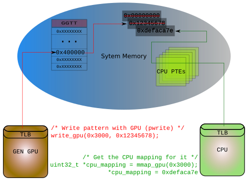
Each element within the GTT is an entry, and the initialism for each entry is a, "PTE" or page table entry. Much of the required initialization is handled by the boot firmware. The i915 driver will get any required information from the initialization process via PCI config space, or MMIO.
Location
The table is located within system memory, and is allocated for us by the BIOS or boot firmware. To clarify the docs a bit, GSM is the portion of stolen memory for the GTT, DSM is the rest of stolen memory used for misc things. DSM is the tolen memory referred to by the current i915 code as "stolen memory." In theory we can get the location of the GTT from MMIO MPGFXTRK_CR_MBGSM_0_2_0_GTTMMADR (0x108100, 31:20), but we do not do that. The register space, and the GTT entries are both accessible within BAR0 (GTTMMADR).
All the information can be found in Volume 12, p.129: UNCORE_CR_GTTMMADR_0_2_0_PCI. Quoting directly from the HSW spec,
The range requires 4 MB combined for MMIO and Global GTT aperture, with 2MB of that used by MMIO and 2MB used by GTT. GTTADR will begin at GTTMMADR 2 MB while the MMIO base address will be the same as GTTMMADR.
In the below code you can see we take the address in the PCI BAR and add half the length to the base. For all modern GENs, this is how things are split in the BAR.
/* For Modern GENs the PTEs and register space are split in the BAR */
gtt_phys_addr = pci_resource_start(dev->pdev, 0) +
    (pci_resource_len(dev->pdev, 0) / 2);

dev_priv->gtt.gsm = ioremap_wc(gtt_phys_addr, gtt_size);
One important thing to notice above is that the PTEs are mapped in a write-combined fashion. Write combining makes sequential updates (something which is very common when mapping objects) significantly faster. Also, the observant reader might ask, 'why go through the BAR to update the PTEs if we have the actual physical memory location.' This is the only way we have to make sure the GPUs TLBs get synchronized properly on PTE updates. If this weren't required, a nice optimization might be to update all the entries as once with the CPU, and then go tell the GPU to invalidate the.
Size
Size is a bit more straight forward. We just read the relevant PCI offset. In the docs: p.151 GSA_CR_MGGC0_0_2_0_PCI offset 0x50, bits 9:8
And the code is even more straightforward.
static inline unsigned int gen6_get_total_gtt_size(u16 snb_gmch_ctl)
{
        snb_gmch_ctl >>= SNB_GMCH_GGMS_SHIFT;
        snb_gmch_ctl &= SNB_GMCH_GGMS_MASK;
        return snb_gmch_ctl << 20;
}
pci_read_config_word(dev->pdev, SNB_GMCH_CTRL, &snb_gmch_ctl);
gtt_size = gen6_get_total_gtt_size(snb_gmch_ctl);
gtt_total = (gtt_size / sizeof(gen6_gtt_pte_t)) << PAGE_SHIFT;
Layout
The PTE layout is defined by the [PRM] and as an example, can be found on page 35 of [HSW] - Volume 5: Memory Views. For convenience, I have reconstructed the important part here:
| 31:12 | 11 | 10:04 | 03:01 | 0 |
|---|---|---|---|---|
| Physical Page Address 31:12 | Cacheability Control[3] | Physical Page Address 38:32 (Previous gens went to 39) | Cacheability Control[2:0] | Valid |
The valid bit is always set for all GGTT PTEs . The programming notes tell us to do this (also on page 35 of HSW - Volume 5: Memory Views) ((I have submitted two patch series, one of which has been reverted, the other, never merged, which allow invalid PTEs for debug purposes)).
Putting it together
As a result, of what we've just learned, we can make up a function to write the PTEs.:
/**
 * gen_write_pte() - Write a PTE entry
 * @dev_priv:   The driver private structure
 * @address:    The physical address to back the graphics VA
 * @entry:  Which PTE in the table to update
 * @cache_type: Preformatted cache type. Varies by platform
 */
static void
gen_write_pte(dev_priv, phys_addr_t address,
          unsigned int entry, uint32_t cache_type)
{
    /* Total size, divided by the PTE size is the max entry */
    BUG_ON(entry >= (gtt_total / 4);
    /* We can only use 38 address bits */
    BUG_ON(address >= (1<<39);

    uint32_t pte = lower_32_bits(address) |
               (upper_32_bits(address) << 4) |
               cache_type |
               1;
    iowrite32(pte, dev_priv->gtt.gsm + (entry * 4));
}
Example
Let's analyze a real HSW running something. We can do this with the tool in the intel-gpu-tools suite, intel_gtt, passing it the -d option (intel_gtt is currently not supported for GEN8+. If someone wants to volunteer to update this tool for gen8, please let me know).
| GTT offset | PTEs |
|---|---|
| 0x000000 | 0x0ee23025 0x0ee28025 0x0ee29025 0x0ee2a025 |
| 0x004000 | 0x0ee2b025 0x0ee2c025 0x0ee2d025 0x0ee2e025 |
| 0x008000 | 0x0ee2f025 0x0ee30025 0x0ee31025 0x0ee32025 |
| 0x00c000 | 0x0ee33025 0x0ee34025 0x0ee35025 0x0ee36025 |
| 0x010000 | 0x0ee37025 0x0ee13025 0x0ee1a025 0x0ee1b025 |
| 0x014000 | 0x0ee1c025 0x0ee1d025 0x0ee1e025 0x0ee1f025 |
| 0x018000 | 0x0ee80025 0x0ee81025 0x0ee82025 0x0ee83025 |
| 0x01c000 | 0x0ee84025 0x0ee85025 0x0ee86025 0x0ee87025 |
And just to continue beating the dead horse, let's breakout the first PTE:
| 31:12 | 11 | 10:04 | 03:01 | 0 |
|---|---|---|---|---|
| Physical Page Address 31:12 | Cacheability Control3 | Physical Page Address 38:32 | Cacheability Control2:0 | Valid |
| 0xee23000 | 0 | 0x2 | 0x2 | 1 |
Physical address: 0x20ee23000 Cache type: 0x2 (WB in LLC Only – Aged "3") Valid: yes
Definition of a GEM BO
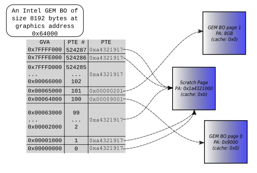
We refer to virtually contiguous locations which are mapped to specific graphics operands as one of, objects, buffer objects, BOs, or GEM BOs.
In the i915 driver, the verb, "bind" is used to describe the action of making a GPU virtual address range point to the valid backing pages of a buffer object. (I've fought to call this operation, "map") The driver also reuses the verb, "pin" from the Linux mm, to mean, prevent the object from being unbound.
Scratch Page
We've already talked about the scratch page twice, albeit briefly. There was an indirect mention, and of course in the image directly above. The scratch page is a single page allocated from memory which every unused GGTT PTE will point to.
To the best of my knowledge, the docs have never given a concrete explanation for the necessity of this, however one might assume unintentional behavior should the GPU talk a page fault. One would be right to interject at this point with the fact that by the very nature of DRI drivers, userspace can almost certainly find a way to hang the GPU. Why should we bother to protect them against this particular issue? Given that the GPU has undefined (read: Not part of the behavioral specification) prefecthing behavior, we cannot guarantee that even a well behaved userspace won't invoke page faults (Empirically (for me), GEN7+ GPUs have behaved themselves quite well after taking the page fault. I very much believe we should be using this feature as much as possible to help userspace driver developers).
Correction: after writing this, I went and looked at the docs. They do explain exactly which engines can, and cannot take faults. The "why" seems to be missing however.
Mappings and the aperture
First we need to take a bit of a diversion away from GEN graphics (which to repeat myself, are all of the shared memory type). If one thinks of traditional discrete graphics devices, there is always embedded GPU memory. This poses somewhat of an issue given that all end user applications require the CPU to run. The CPU still dispatches work to the GPU, and for cases like games, the event loop still runs on the CPU. As a result, the CPU needs to be able to both read, and write to memory that the GPU will operate on. There are two common solutions to this problem.
- DMA engine
- Setup overhead.
- Need to deal with asynchronous (and possibly out of order) completion. Latencies involved with both setup and completion notification.
- Need to actually program the interface via MMIO, or send a command to the GPU (I've previously written a post) on how this works for Intel).
- Unlikely to re-arrange or process memory
- tile/detile surfaces (Sorry people, this one is too far out of scope for and explanation in this post. Just trust it's a limitation if you don't understand.
- can't take page faults, pages must be pinned
- No size restrictions (I guess that's implementation specific)
- Completely asynchronous - the CPU is free to do whatever else needs doing.
- Setup overhead.
- Aperture
- Synchronous. Not only is it slow, but the CPU has to hand hold the data transfer.
- Size limited/limited resource. There is really no excuse with PCIe and modern 64b platforms why the aperture can't be as large as needed, but for Intel at least, someone must be making some excuses, because 512MB is as large as it gets for now.
- Can swizzle as needed (for various tiling formats).
- Simple usage model. Particularly for unified memory systems.
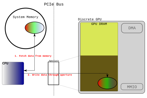
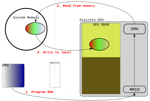
The Intel GEN GPUs have no local memory (There are several distinct caches on all modern GEN GPUs, as well as eDRAM for Intel's Iris Pro. The combined amount of this "local" memory is actually greater than many earlier discrete GPUs). However, DMA has very similar properties to writing the backing pages directly on unified memory systems. The aperture is still used for accesses to tiled memory, and for systems without LLC. LLC is out of scope for this post.
GTT and MMAP
There are two distinct interfaces to map an object for reading or writing. There are lots of caveats to the usage of these two methods. My point isn't to explain how to use them libdrm is a better way to learn to use them anyway). Rather I wanted to clear up something which confused me early on.
The first is very straightforward, and has behavior I would have expected.
struct drm_i915_gem_mmap {
#define DRM_I915_GEM_MMAP       0x1e
    /** Handle for the object being mapped. */
    __u32 handle;
    __u32 pad;
    /** Offset in the object to map. */
    __u64 offset;
    /**
     * Length of data to map.
     *
     * The value will be page-aligned.
     */
    __u64 size;
    /**
     * Returned pointer the data was mapped at.
     *
     * This is a fixed-size type for 32/64 compatibility.
     */
    __u64 addr_ptr;
};

// let bo_handle = some valid GEM BO handle to a 4k object
// What follows is a way to map the BO, and write something
memset(&arg, 0, sizeof(arg));
arg.handle = bo_handle;
arg.offset = 0;
arg.size = 4096;
ioctl(fd, DRM_IOCTL_I915_GEM_MMAP, &arg);
*((uint32_t *)arg.addr_ptr) = 0xdefecate;
I might be projecting my ineptitude on the reader, but, it's the second
interface which caused me a lot of confusion, and one which I'll talk briefly
about. The interface itself is even simpler smaller:
#define DRM_I915_GEM_MMAP_GTT   0x24
struct drm_i915_gem_mmap_gtt {
    /** Handle for the object being mapped. */
    __u32 handle;
    __u32 pad;
    /**
     * Fake offset to use for subsequent mmap call
     *
     * This is a fixed-sizeso [sic] type for 32/64 compatibility.
     */
    __u64 offset;
};
Why do I think this is confusing? The name itself never quite made sense - what use is there in mapping an object to the GTT? Furthermore, how does mapping it to the GPU allow me to do anything with in from [userspace]. For one thing, I had confused, "mmap" with, "map." The former really does identify the recipient (the CPU, not the GPU) of the mapping. If follows the conventional use of mmap(). The other thing is that the interface has an implicit meaning. A GTT map here actually means a GTT mapping within the aperture space. Recall that the aperture is a subset of the GTT which can be accessed through a PCI BAR. Therefore, what this interface actually does is return a token to [userspace] which can be [mmap'd] to get the CPU mapping (through the BAR, to the GPU memory). Like I said before, there are a lot of caveats with the decisions to use one vs. the other which depend on platform, the type of surface you are operating on, and available aperture space at the time of the call. All of these things will not be discussed.
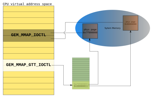
Finally, here is a snippet of code from intel-gpu-tools that hopefully just encapsulates what I said and drew.
mmap_arg.handle = handle;
assert(drmIoctl(fd, DRM_IOCTL_I915_GEM_MMAP_GTT, &mmap_arg) == 0);
assert(mmap64(0, OBJECT_SIZE, PROT_READ | PROT_WRITE, MAP_SHARED, fd, mmap_arg.offset));
Summary
This is how modern Intel GPUs deal with system memory on all platforms without a PPGTT (or if you disable it via module parameter). Although I happily skipped over the parts about tiling, fences, and cache coherency, rest assured that if you understood all of this post, you have a good footing. Going over the HSW docs again for this post, I am really pleased with how much Intel has improved the organization, and clarity. I highly encourage you to go off and read those for any missing pieces.